
Adani University plans to develop capabilities in semiconductor design, manufacturing and packaging at its upcoming multidisciplinary campus in Ahmedabad, as it seeks to strengthen the link between higher education, research and industrial applications.
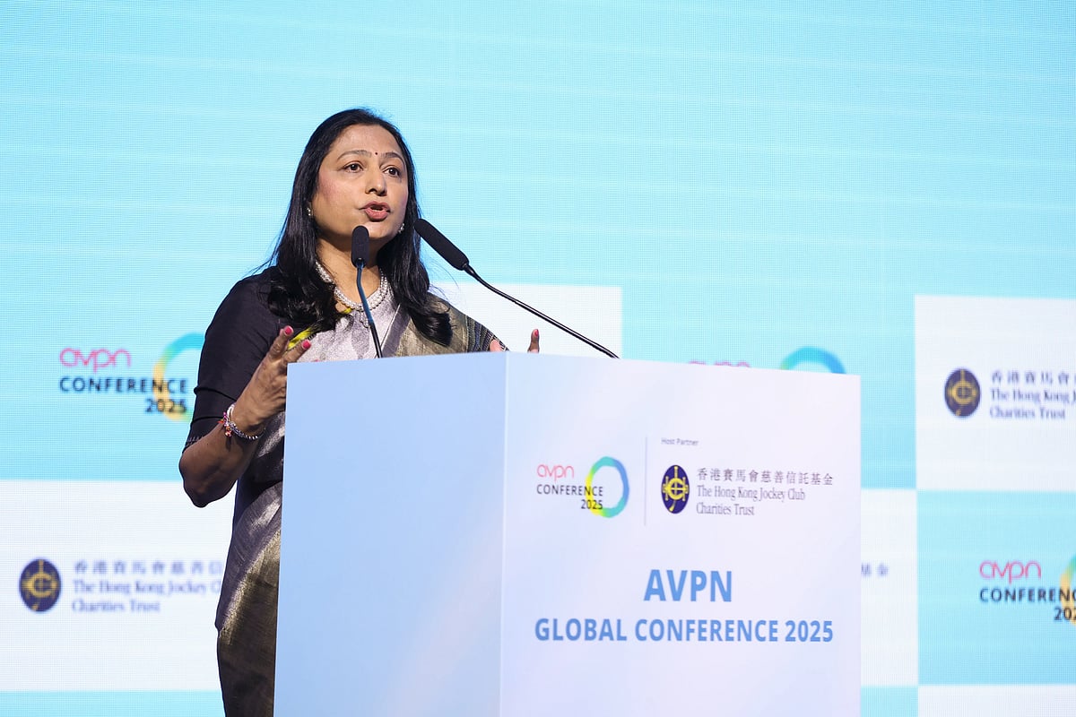
Dr. Priti Adani, President of Adani University and the Adani Institute of Digital Technology Management (AIDTM), said the proposed campus would focus on bringing education, research and industry together to address real-world challenges.
“As we develop our new world-class multidisciplinary global campus in Ahmedabad, our ambition is to bring education, research, and industry together to solve real-world problems,” Dr. Adani said.
The proposed focus on semiconductors places industry-oriented skill development among the priorities outlined for the campus. The plans cover design, manufacturing and packaging, three areas of the semiconductor value chain that require specialised technical expertise.
Adani said the institution’s ambition extended beyond developing physical infrastructure, with an emphasis on building the capabilities of faculty members, industry professionals and young engineers.
“While facilities in an institution are important, it is the people within the institution that truly strengthen it,” she said.
The university intends to offer advanced executive education for industry professionals, faculty development initiatives and specialised programmes for young engineers, according to her statement.
These initiatives are intended to build the depth of knowledge and technical skills India will need over the coming decades. The emphasis on executive education also points to a focus on upgrading the capabilities of professionals already working in industry, alongside training new entrants.
Developing expertise across semiconductor design, manufacturing and packaging would require specialised training and closer interaction between academic institutions and industry. Adani’s remarks signal an ambition to incorporate these requirements into the institution’s academic and research agenda.
The proposed multidisciplinary approach seeks to connect classroom learning with practical applications, potentially creating opportunities for industry collaboration and research-led problem-solving.
However, the statement did not specify the campus investment, project timeline, planned student capacity or the scale of the proposed semiconductor programmes. Details of potential industry partnerships and the infrastructure to support semiconductor-related research were also not provided.
Dr. Adani indicated that the institution’s ambitions extended further, although the statement shared did not include details of those additional plans.